PHYSICS
УДК 621.315.592
Academician E. М. Кazaryan1, А. А.
Кostanyan1, H. A. Sarkisyan*1,2
Optical absorption in GaAs quantum well caused by
donor-acceptor
pair transitions
(Submitted 20/IX/06)
Keywords: quantum well, donor-acceptor pair, transitions
1. Introduction. The investigation of
properties related with impurity centers in semiconductor quantum well (QW)
structures has not only fundamental interest, but also is of major importance in
optoelectronic device applications (high electron mobility transistors, QW
infrared photodetectors or emitters, etc.) [1].
In semiconductors of A3B5 group, the electrons
that bound with doped impurities, form shallow energy states close to band gap
edges. In particular, doping the bulk semiconductor simultaneously with both
donor and acceptor impurities, form the shallow states near the band gap edges,
making possible optical transitions between two clearly isolated energy levels.
[2-4].
One of the first works related to
investigations of donor-acceptor pair (DAP) transitions in above- mentioned
semiconductors is Hopfield's work [2]. Later, detailed investigation of DAP
transitions were made by Stoneham and Harker [3], where central-cell corrections
were taken into account.
The investigation of
hydrogenic impurities in GaAs QW was in details performed by Bastard [5]. Later
investigations of impurity properties in QW was followed by several other, more
detailed investigations. The energy spectrum of the ground state and the
low-lying excited states for shallow impurities in QW structures, influence of
dielectric constant mismatches at well interfaces, effects of spatially
dependent screening, electron-phonon interactions, nonparabolicy of the
conduction and valence band, etc. were in details performed by other authors
(see for example Ref. [6])
Variations in the
properties can be caused by changing the concentration of the dopant from
uniform distributions within QW to concentrated sheet layers resulting in a
so-called d-doped profile. Energetic levels of an
impurity are possible to tune in a controlled way by changing the doping
profile. Understating the influence of impurities on the optical properties near
the QW intrinsic transitions is of particular concern in order to optimize the
design of optoelectronic devices.
The PL
spectrum is an effective technique for characterizing doped QWs. In addition to
free-excitonic transition, donor-bound exciton [7,8], acceptor-bound exciton
[9], free electron to acceptor [10-12] and heavy hole to donor [10-12]
transitions were also observed in p-type and n-type doped
QWs.
Besides above-mentioned ones,
acceptor-to-donor pair transitions in QWs are also possible. There are several
experimental reports concerning observation of the DAP transition peak in the PL
spectra. Ding et al [13] have reported an observation of an anomalously large
blueshift of apparent DAP transition peak in compensation-doped coupled QWs. The
blueshift was observed in PL spectra while the excitation intensity increases
from 0.54 to 423 W/cm2. Authors proposed that the blueshift is due to
the change of the Coulomb interaction energy between recombined donors and
acceptors as their separation decreases. Later Guzman et al [14] performed an
optical characterization of GaAs/GaAlAs single QW structures by interband PL
spectroscopy. The peak in PL spectra at lower energy was observed and attributed
to DAP transition. Samples were grown by molecular beam epitaxy (MBE) with
two-dimensional doping concentration (Si) in the wells in the range of
0-1012 cm-2. Si is related to
acceptor, while C is related to residual donor, which is always present in
samples grown by MBE. In this connection, one can assume that non-compensated
QWs were considered. The dependence of DAP transition peak on different doping
concentration was performed, and the blueshift was
observed.
However, in above-mentioned
experimental works, discussions about DAP transitions concerned only qualitative
aspect of the subject. In this connection, it is important to have a
quantitative model, which will describe aforementioned transitions that can give
an opportunity to perform an essential comparison between theory and the
experiment.
In this paper, we present a
theoretical investigation of DAP transitions in the framework of non-compensated
lightly doped GaAs infinite-barrier QW.
2.
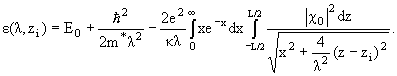
Theory. The impurity envelope functions are the solutions of Schr
ödinger
equation with the effective Hamiltonian
|
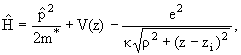
|
(1) |
where m* is the electron
effective mass, к - the dielectric constant (for GaAs к = 13.18), zi
(i = D, A) is the impurity position along OZ axes, V(z) - the confinement
potential.
For definiteness we will only
refer to the donor state, because it is clear that (1) also applies to the
acceptor state, where m* understood as the hole effective
mass.
We present the envelope function of
ground state as
where j0(r) is the function in
QW plane and c0(z) is along the quantization
axis OZ.
Taking into account the
normalization condition for c0(z) we get
two-dimensional Schr | ödinger
equation for the function j0(r)
|
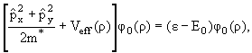
|
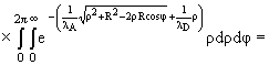
(3) | where Veff (r) is the effective Coulomb potential in XOY plane:
|
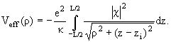
|
(4) | The
solution of Eq.(3) is found using the variational method, with the trial
function of the ground state in the form [5]
|
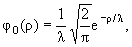
|
(5) | where l is
the variational parameter.
The ground state
energy is obtained after the minimization of the function
|
|
(6) | The
binding energy is equal to
|
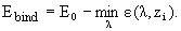
|
(7) |
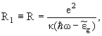
Now
we turn to the calculation of the absorption coefficient in considered
structure, conditioned by transitions between ground states of
DAP.
Let us consider lightly doped QW with
concentration of acceptors nA, so that
 >> aD,aA conditions are satisfied
 is the average distance between acceptors and donors in
the QW plane). In this case the main contribution into the transitions within
the donor-acceptor system makes pairs satisfying to R і
aD,aA conditions, because the number of pairs with R <
aD is not significant. For this case the coupling energy of the DAP
can be taken equal to e2/кR and considered as an
acceptor energy level shift. The location of the donor is
is the average distance between acceptors and donors in
the QW plane). In this case the main contribution into the transitions within
the donor-acceptor system makes pairs satisfying to R і
aD,aA conditions, because the number of pairs with R <
aD is not significant. For this case the coupling energy of the DAP
can be taken equal to e2/кR and considered as an
acceptor energy level shift. The location of the donor is
 and the acceptor is and the acceptor is where
where |
 is the radius vector and is the radius vector and |
 is the
distance between donor and acceptor in QW plane. Later we will assume that donor
and acceptor are located in the center of QW. is the
distance between donor and acceptor in QW plane. Later we will assume that donor
and acceptor are located in the center of QW.
The electron and hole ground eigenstates and eigenvalues are (measured
from the maximum of valence band)
|
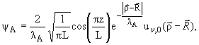
|
(8) |
|
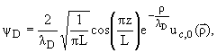
|
(9) |
| EA = - |
min
|
eA(lA) - |
e2
кR
|
, | |
(10) |
where lA, lD are
variational parameters, uv,0, uc,0 - Bloch amplitudes in
the center of the Brillouin zone (in the discussed structure zone extrema are on
the center of Brillouin zone).
The light
absorption coefficient is determined by the formula [15]
| aR(w) = |
4p2c
NwV
|
|
|MAD|2
|A0|2
|
d(Ef - Ei - ħw), | |
(12) |
where V is the sample volume,
MAD - the matrix element of "acceptor®donor"
transition, N - the refractive index, A0 is the vector potential
amplitude of incident electromagnetic wave.
In the case of normal incident light the matrix element can be written
as
| MAD = |
2e
pm0
|
 |
1
lalD
|
2
L
|
-L/2
у
х
L/2
|
eiqzz cos |
ж
з
и |
pz
L
|
ц
ч
ш |
cos |
ж
з
и |
pz
L
|
ц
ч
ш |
dz × | |
 |
2e
pm0
|
|
1
lAlD
|
F(R)x(qzL), | |
where | 
| is
the matrix element conditioned by Bloch amplitudes, |  is the
incident light polarization, qz is the photon wave vector in the z
direction.
is the
incident light polarization, qz is the photon wave vector in the z
direction.
By F(R) and x(qzL) we denoted the following integrals
| x(qzL) = |
2
L
|
|
L/2
у
х
-L/2
|
eiqzz cos |
ж
з
и |
|
pz
L
|
|
ц
ч
ш |
cos |
ж
з
и |
|
pz
L
|
|
ц
ч
ш |
dz. | |
In discussed case of shallow impurities Eq.(13) can be simplified, if we
take into consideration the fact, that for GaAs
 |
≳ | eg ~ 1 eV (the expression for
see below) and for QW width we have
L ~ 10-6 cm ( ~ 100 | Å),
which makes the parameter qzL << 1. This allows us to take
x(qzL) approximately equal to
1.
As it follows from Eq. (12) such
transitions are possible only between those DAPs, the distances between which
can be determined from the energy conservation law
|
 |
(15) | where
|
 |
(16) | Considering R as changing continuously when nA >>
nD, let us write the expression for the absorption coefficient [4]
| a(w) = ND |
Ґ
у
х
0
|
aR(w)W(R)dR, | |
(17) | where ND - number of
donors, W(R) - distribution function by R values.
As DAPs distribution function we take the adjacent-neighbor distribution
[4], and taking W(R) not dependent on z:
| W(R) = 2pRnAexp{-pR2LnA}, | |
(18) | where nA is the bulk
concentration of acceptors.
After averaging
over the distribution (18) for the absorption coefficient of DAP transition we
obtain the following expression
|
 |
(19) |
where
 and and
 are two dimensional
surface concentrations of acceptors and donors,
respectively. are two dimensional
surface concentrations of acceptors and donors,
respectively.
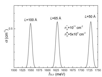
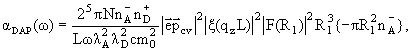
3. Discussion. Fig. 1 shows the
dependencies of the absorption coefficient on the energy of incident light at
different values of QW width (L = 50 | Å,
65 | Å,
100 | Å). As
it follows from figure, with the increase of L the effective width of the
forbidden band decreases and therefore the absorption threshold shifts to the
smaller energies (smaller frequencies), as a result of size-quantization
weakening. Also small reduction of the absorption coefficient value is observed.
Calculations are made at the value of dominant impurity (acceptors)
concentration equals to
= 1011 cm-2, and at k = 0.05 compensation value
(k = The numerical values of parameters in the
absorption coefficient (19) in the GaAs structures are: egap = 1.519 eV, mn = 0.34me, mc = 0.067me,
N = 3.6.
Fig.1. Absorption coefficient dependence on incident light
frequency at different widths of QW The numerical values of parameters in the
absorption coefficient (19) in the GaAs structures are: egap = 1.519 eV, mn = 0.34me, mc = 0.067me,
N = 3.6.
Fig.1. Absorption coefficient dependence on incident light
frequency at different widths of QW
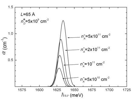
Fig. 2 presents the absorption coefficient
dependencies on the incident light frequency at different values of dominant
impurity concentration
 = 5 × 1010 cm-2,
= 1011 cm-2,
= 2 × 1011 cm-2,
= 5 × 1011 cm-2). With the increase of the impurity concentration
the absorption coefficient growth occurs, as well as threshold frequency
slightly increases (i.e. the blueshift is observable).
= 5 × 1010 cm-2,
= 1011 cm-2,
= 2 × 1011 cm-2,
= 5 × 1011 cm-2). With the increase of the impurity concentration
the absorption coefficient growth occurs, as well as threshold frequency
slightly increases (i.e. the blueshift is observable).
Fig.2. Absorption coefficient dependence on incident light
frequency at different concentrations of dominant
impurity
Fig. 3 shows the blueshift dependences on different
values of two-dimensional concentrations of dominant impurity (acceptor). There is a
significant difference between the experimental and theoretical data for the lightly
doped samples.
Fig.3. The blueshift dependence on dominant impurity
(acceptor) concentration: squares - experimental
results29, solid line - result
of calculations, left - region of low concentrations, right - region of high
concentrations The blueshift
can be presented as
| DEshift = eg - EbD - EbA + |
q1q2
R
|
| |
(20) |
where EbD and
EbA are donor and acceptor binding energies, respectively; the fourth
item in Eq.(20) is the Coloumbian term. When acceptor concentration is
increasing (e.g. concentration of Si atoms [14]), donors (e.g. residual C atoms
[14]) and acceptors become spatially closer, the blueshift in the acceptor-donor
transition peak should take place, as a result of the Coloumbian term increase
[13], [14]. So the growth of doping level should be the reason of blueshift
increase. Such a result is obtained in our theoretical
model.
In Ref.[14] the blueshift of DAP
transition peak was observed with respect to e1-hh1 peak (transition between
first conduction subband and first heavy-hole subband) in GaAs/AlGaAs QW
infra-red detector structures. The considered samples with different
concentrations of impurities were grown at different runs via MBE. In the
reported results fluctuations of QW thicknesses (appearing due to different
runs) introduce certain variation into blueshift growth tendency along with
impurity concentration growth in the lightly doping samples. The comparison of
our theoretical results with the experimental data shows that in the lightly
doped samples the mentioned technological fluctuations significantly affect on
the blueshift growth tendency along with the impurity concentration increase
from sample to sample. As it is seen from Fig. 1, even small differences in well
thicknesses can result in significant shift of the absorption threshold (peak
position).
4. Conclusion. We have presented
the theoretical model for donor-acceptor pair transitions in non-compensation
doped GaAs QW. These transitions are taking place between different impurity
atoms' levels. The developed model enables in the frames of simple theoretical
model to simulate blueshift behavior in doped QW
structures.
This work was supported by the
Armenian State Program "Semiconductor Nanoelectronics".
1Russian-Armenian State
University
2Yerevan State
University
*Corresponding author:
e-mail address: shayk@ysu.am; tel.: +374 10 553-246
Литература
1. B. F. Levine - Journ. Appl.
Phys. 1993. V. 74. R1-81.
2. J. J. Hopfield
- Proc. Int. Conf. on Semiconductors. Paris. 1964. P. 725.
3. A. M. Stoneham, A. H. Harker - Journ. Phys. C: Solid St. Phys. 1975. V. 8. P. 1109-18.
4. E. M. Kazaryan, A. H. Melikyan, H. R.
Minasyan - Sov. Phys. Semiconductors. 1979. V. 13. P. 2034.
5. G. Bastard - Phys. Rev.
1981. B 24. P. 4714.
6. S. Frazzoli, F.
Bassani, R. Buczko - Phys. Rev. 1990. B 41. P. 5096.
7. R. Stepniewski, S. Huant, G. Martinez,
B. Etienne - Phys. Rev. 1989. B 40. P. 9772.
8. P. O. Holtz, B. Monemar, M. Sundaram, J. L. Merz, A. C. Gossard
- Superlatt. Microstruct. 1992. V. 12. P. 133.
9. Q. X. Zhao, P. O. Holtz, C. I. Harris,
B. Monemar, E. Veje - Appl. Phys. Lett. 1994. V. 64. P. 2721.
10. L. E. Oliveira, R. Perez-Alvarez -
Phys. Rev. 1989. B 40. P. 10460.
11. E. M. Kazaryan, A. A. Kostanyan, H. A. Sarkisyan - Physica. 2005. E 28. P. 423.
12. J. Kundrotas, A. Cerskus, S. Asmontas, G. Valusis, B. Sherliker, M. P. Halsall, M.
J. Steer, E. Johannessen, P. Harrison - Phys. Rev. 2005. B 72. P.
235322.
13. Y. J. Ding, R. Korotkov, J. B.
Khurgin, W. S. Rabinovich, D. S. Katzer - Appl. Phys. Lett. 1998.
V. 72. P. 534.
14. A. Guzman, J. L.
Sanchez-Rojas, J. M. G. Tijero, J. J. Sanchez, J. Hernando, E. Calleja, E.
Mufioz, G. Vergara, M. T. Montojo, L. J. Gornez, P. Rodriiguez, R. Alrnazan, M.
Verdu - IEE Proc.-Optoelectron. 1999. V. 146. P. 89.
15. А. I. Anselm - Introduction of Semiconductors Theory. Nauka. 1978. in Russian.
|